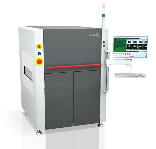
ASMPT Process Lens 5D Solder Paste inspection System - MORE PRECISION, SPEED,AND INVESTMENT PROTECTION
Process Lens is a highly precise, flexible, state-of-the-art 5D inline SPI system with on-the-fly 3D compensation of PCB warping. It is fast enough even for inline measurements with dual conveyors. Thanks to its smart algorithms, the Process Lens understands what it measures and knows how to interpret the results accordingly. It measures what matters: solder paste deposits, glue, contaminations, dust, and more – all while suppressing any measurement noise generated by the circuit board.
The choice is yours: the Process Lens has a DLP chip with 8 million individually controllable micromirrors and a scanning field of 30 x 30 millimeters, while the Process Lens HD features 20 million micromirrors and a scanning field of 50 x 50 millimeters. The Process Lens HD is up to 70 percent faster than traditional systems while maintaining a very high measurement accuracy, but with 80 percent fewer false calls. It also offers full flexibility, where users can switch between high-speed and high-resolution modes through software.
The bottom line: more stable printing processes, higher throughput rates, and significantly better yields. Unmatched and unbeatable by the competition – compare for yourself.
The future awaits - Smart process optimization that’s easy to retrofit
Absolutely unique: With the optional WORKS Process Expert software you can upgrade your 5D SPI to the world’s first self-learning inline expert system for optimizing your printing process.
The WORKS Process Expert Printing Solution optimizes your printing process proactively with virtual prints, trend analyses and direct DEK printer control – optionally fully autonomously with no operator assists whatsoever.
The expert software learns from each print cycle 24/7, 365 days a year,and never forgets a detail.
The most Innovative measurement system
Moiré phase shifting with 8 or 20 million
digitally controllable micromirrors
Maximum accuracy
Precise X/Y positioning, combined 2D/3D measurements and on-the-fly compensation of board warpage
Shadow-free
Multiple light sources
Comprehensive
Visualization of position, area, height, volume and shape of all solder deposits;checks for coplanarity and bridging
Maximum throughput Inline measurement in dual-conveyor mode
Easy operation
Quick programming with component library and recommendations of inspection criteria
Investment protection
Software-upgradeable to Process Expert
inline expert system for autonomous process optimization