
Product Code: SPHERE
Designed for wafer processing, Nordson MARCH‘s SPHERE™series plasma systems are ideal for wafer-level and 3D packaging applications. Plasma applications include descum, ashing/photoresist/polymer stripping, dielectric etch, wafer bumping, organic contamination removal, and wafer destress.
Nordson MARCH‘s SPHERE series plasma systems are ideal for wafer processing prior to typical back-end packaging steps, as well as wafer fan out, wafer-level packaging, 3D packaging, flip-chip, and traditional packaging. The patented chamber design and control architecture enables short plasma cycle times with very low overhead, ensuring that throughput for your application is maximized and cost of ownership is minimized.
SPHERE series systems support automated handling and processing of round or square wafer/substrate sizes ranging from 75mm to 300mm. In addition, thin wafer processing with or without carriers is possible, depending upon wafer thickness.
The patented plasma chamber design provides exceptional etch uniformity and process repeatability. Primary plasma applications include a variety of etching, ashing, and descum steps. Other plasma processes include contamination removal, surface roughening, increasing wettability, and enhancing bonding and adhesion strength, photoresist/polymer stripping, dielectric etch, wafer bumping, organic contamination removal, and wafer destress.
Wafer Cleaning - The SPHERE series plasma systems remove contamination prior to wafer bumping, remove organic contamination, remove fluorine and other halogen contamination, and remove metal and metal oxides. Plasma also improves spun-on film adhesion and cleans metallic bond pads.
Wafer Etching - Plasma systems descum wafer of residual photoresist and BCB, pattern dielectric layers for redistribution, strip/etch photoresist, enhance adhesion of wafer applied materials, remove excess wafer applied mold /epoxy, enhance adhesion of gold solder bumps, destress wafer to reduce breakage, improve spun-on film adhesion, and clean aluminum bond pads.
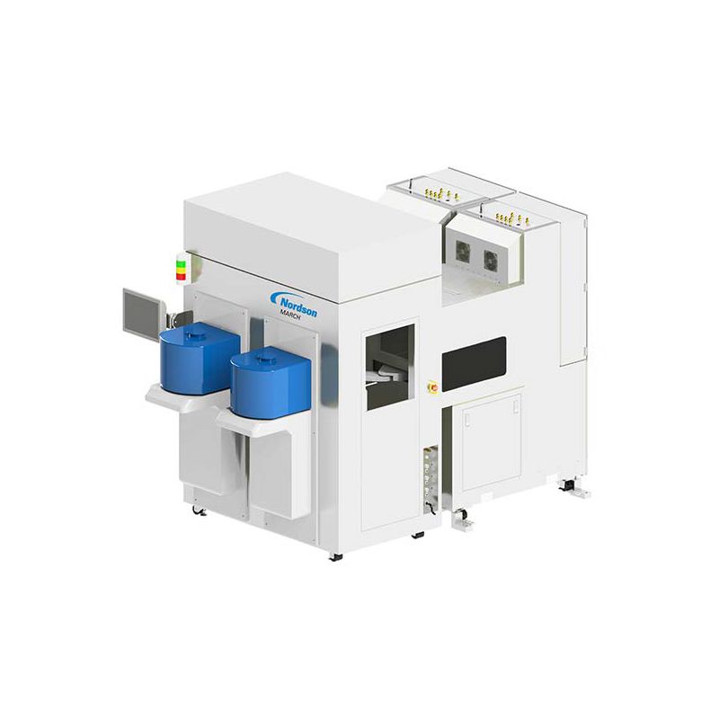
Models and ConfigurationsStratoSPHERE™ Plasma System: Designed for high-throughput processing of semiconductor wafers up to 300mm (12 in.) in diameter. The patented plasma chamber design provides exceptional etch uniformity and process repeatability. Its three-axis symmetrical chamber ensures all areas of the wafer are treated uniformly, while tight control over all process parameters ensures highly repeatable results.